QFN Package Simulation
he Quad Flat No-lead (QFN) package is a CSP (plastic encapsulated package) with a copper lead frame substrate. QFN type package is one of the most cutting-edge IC packaging technologies in the electronics. The QFN is a leadless package where electrical contact to the PCB is made by soldering the leads on the bottom surface of the package to the PCB, instead of the conventional formed perimeter gull wing leads.
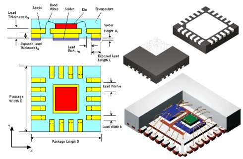 The QFN-type package is known for its small size, cost-effectiveness and good production yields. QFN also possess certain mechanical advantages for high-speed circuits including improved co-planarity and heat dissipation. The QFN has pins on 4 edges of the bottom surface of the package. The QFN can have either a square or rectangle body as well as symmetric or asymmetric terminal patterns. The QFN was introduced to replace the gull wing lead Quad Flat Package (QFP) because the component leads are embedded in the plastic and cannot be bent during handling to insure consistent assembly attachment.
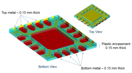 4×4 [mm] 16 Pin QFN
Design is shown below . This QFN package has 16 pin. Metal thickness is 0.15 mm and plastic encasement is 0.15 thick. Defining a substrate stack up for QFN is pretty straightforward. The mold encapsulations are defined by dielectric bricks and the leads are defined by vias. The top side graphic shows the side view of package that is mounted on PCB. The bottom picture shows the details of leads, bondwires, and the chip, in this case, a thin film circuit.
QFN Electromagnetic simulation model and result
The input and output transmission lines on the PC board are connected to the package leads. On the top of die paddle, 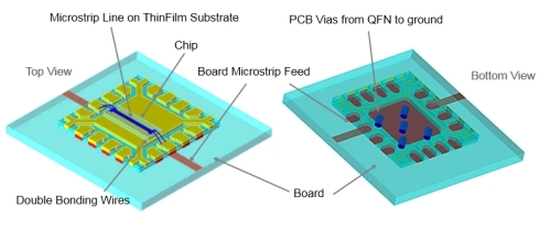 a thin film circuit with a thru transmission line is attached to see the package performance. Double bonding with a compensated bond pads are used to improve the frequency performance here. With this typical interconnect scheme, the simulation results show that the package can be used up to
 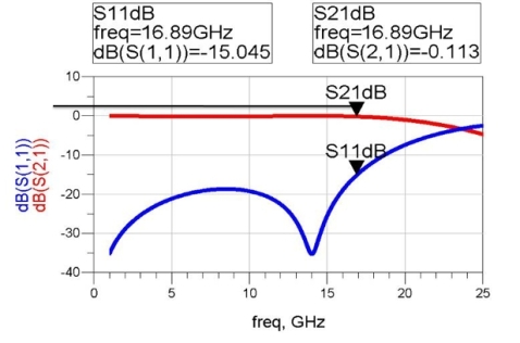 15GHz when the required input and output return loss are around -20dB.
a thin film circuit with a thru transmission line is attached to see the package performance. Double bonding with a compensated bond pads are used to improve the frequency performance here. With this typical interconnect scheme, the simulation results show that the package can be used up to 15GHz when the required input and output return loss are around -20dB.
Package performance can be further improved by Increasing the width of input/output transmission lines to make 50ohm impedance or use two lead frames instead of single to minimize the transitional impedance profile and split the double bonding to the two lead frames.

generally the PCB trace would be wider than the QFN lead, what's ur take on the mismatch caused by it
ReplyDelete