Posts

Showing posts with the label EMPro

EMI & EMC Compliance of Smartphone

EMC within electronic components has become an increasingly important issue for embedded designers to contend with. As system frequencies and the need for lower supply voltages increase, the end application becomes more and more vulnerable to the negative affects of EMI. These electrical influences can be generated by either radiated or conductive EMI sources. Radiated sources include anything electrical or electromechanical, including motors, power lines, antennas, traces on a PCB (Printed Circuit Board), and even the silicon components on the PCB. Conductive EMI primarily shows itself as electrical “noise” on the power supply lines of an application and can be caused by induced voltage spikes from other devices within a system. Electromagnetic Interference (EMI): Electromagnetic emissions from a device or system that  interfere with the normal operation of another device or system. EMI is also referred to as Radio Frequency Interference (RFI) Electromagnetic Compatibilit...
Array Antenna Feed Networks There is various kind of feeding network of an array antenna. Feed network depend on antenna type and geometry. Feed network for microwave applications is a major design concern in terms of complexity and size.

SIW (Substrate Integrated Waveguide) Patch Antena

SIW technology is essentially a hybrid of microstrip and dielectric-filled waveguide (DFW) technologies. Starting with a PCB substrate, top and bottom metal layers provide two of the waveguide walls. Then, two parallel rows of vias are added, forming the side walls of the waveguide. Figure 1 shows a microwave filter constructed using SIW technology. The SIW technology for passive circuit design has been  implemented for its low cost, compact topology and high performance. There has been increasing interest in implementing SIW technology in active circuits and complete systems, including active integrated antennas.
Image
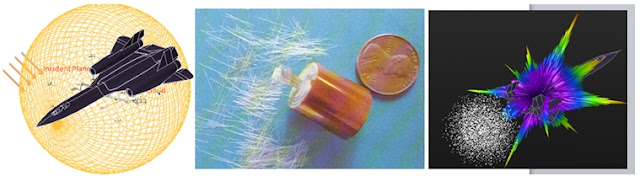
MODELING AND SIMULATION OF CHAFF CLOUD Chaff finds are mainly used in electromagnetic countermeasures. A cloud of chaff is an artificial target made up of a bunch of small thin metallized glass fiber or wire. Chaff consists of thin dipole elements cut to resonate at radar frequencies. Chaff Clouds are dispensed in the air through the chaff cartridge on aircrafts . Chaff Cloud masks the real target return signal therefore, the detection of target become more complicated. The reflected signal from the chaff cloud disturbs the opponent’s radar system and creates a false signature in the enemy radar. Because of high RCS signature, after launching a chaff cloud, the incoming missile tends to track on the chaff. The aircraft can then perform a fast, sharp maneuver, deviating from the missile path. Radar Cross Section (RCS) is defined as the area a target would have to occupy to produce the amount of reflected power that is detected back at the radar, and is classified according ...
Image
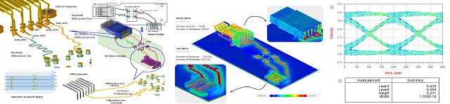
Signal Integrity Analysis of High-Speed Interconnects Signal integrity (SI) addresses two key aspects in high-speed digital designs: signal timing and quality. SI analysis aims to ensure signals reach their destination in good condition. In a system, signals travel through various kinds of interconnections (e.g., from chip to package, package to RF board trace and trace to high-speed connectors), with any electrical impact happening at the source end, along with the transmission path or at the receiving end, which affects both signal timing and quality. Connector performance directly affects system performance and reliability. As a result, designing and modeling connectors for multi-gigabit applications is one of the greatest challenges in high-speed digital applications. When designing high-speed applications, the signal transmission quality is a critical factor. At gigabit speeds, high-speed interconnects must be characterized along with the RF board traces. The ever-increa...

BGA Package Simulation

Image
BGA Package Design and Simulation A BGA package is very popular package style for high speed digital applications due to high density, low thermal resistance, and low inductance leads. In a BGA package, the electrical connections are made of solder balls stuck to the bottom of the package. However as the operating frequency and data rate go up, it is critically important for IC designers to understand the package’s electrical performance because of the parasitics that can come from the package. A package is the second most expensive part next to the silicon and can add 6 to 8 weeks to the cycle time. Given the very tight opportunity window for the majority of digital products, a failure to produce a successful package design can significantly reduce the profit margin or even kill the entire project. Designers are challenged to get the desired package performance right the first time. It requires fast and accurate analysis of BGA packages with EM simulators. A 45 mm pack...

Designing Multilayer Printed Antennas with wide bandwidth

Image
Multi-layer Microstrip Antenna Generally impedance bandwidth of patch antennas varies from 2-3% for single layer direct coupling or probe coupling  and can be further enhanced by coupling the power from the strip line through an aperture (slot) in the ground plane and/or printing patch effectively on the foam material whose dielectric constant is nearly equal to that of air [. In such case the feed network is isolated from the radiating element by a ground plane, which prevents spurious radiation. The resonant or non-resonant slot couples energy from the stripline to the patch. If slot is resonant, it provides another resonance in addition to the patch resonance, resulting in an antenna with 10-15% impedance bandwidth. However, the resonant slot has strong backlobe, which substantially reduces the gain of the antenna. Non-resonant slot has better front to back ratio, which results in improvement in efficiency with narrow bandwidth. Hence multilayer microstrip antennas are di...

How to design SAR antennas

Image
Due to project complexity and cost factor, designer first simulates design using commercial EDA tools to get performance data before real production.  Design cycle time plays a big part in determining a product launch schedule. Companies are under enormous pressure to reduce the time and cost of their design cycle.   Simulation tool capability and the way tools are used, plays important role in design cycle time and cost . There are simulation technologies available that can change the way complex integrated array antenna are designed. One solution enables use of different solvers for radiator and 3D feeder networks separately. This hybrid-design technology reduces total design iteration time significantly. Agilent has three most established EM simulation technologies: Method-of-moments (MoM), finite element method (FEM) and finite difference time domain (FDTD). This paper proposes how to use multiple EM simulation solvers along with other techniques thro...